
A team of Chinese scientists has designed a tiny, modular and revolutionary artificial intelligence (AI) chip based on photonics instead of traditional electronic transistors, paving the way for large-scale photonic computing and efficient real-world AI applications.
The rapid development of AI imposes stringent energy efficiency and area efficiency requirements on next-generation computing. Optical intelligent computing has shown great potential in achieving superior processing speeds and high energy efficiency. This is believed to be a next-generation computing breakthrough that could solve the AI challenges in computing capacity and energy consumption.
However, existing optical computing has failed to realize its full potential for general-purpose intelligent computation. It can only handle simple AI tasks, such as digit classifications or small-scale pattern recognition.
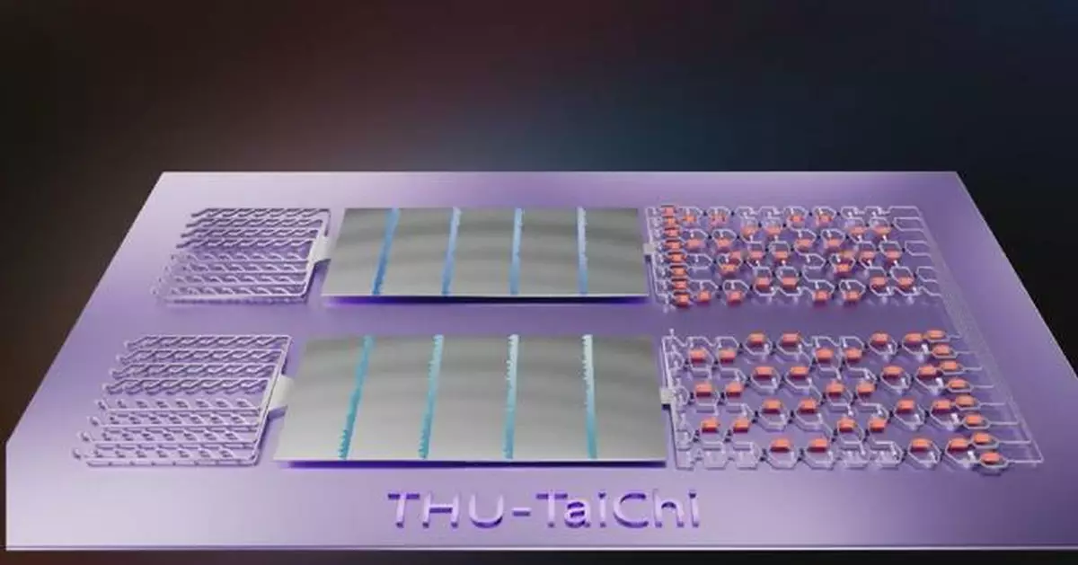
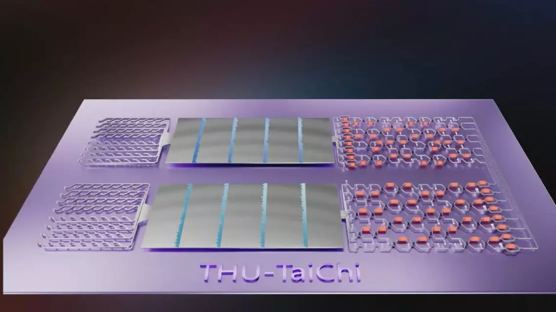
The chip study, published on Friday in the journal Science, reported a large-scale photonic chiplet along with a distributed optical computing architecture named "Taichi."
Developed by researchers from Tsinghua University, Taichi can solve advanced AI tasks with high computing capacity and high energy efficiency.
Instead of going "deeper" as electronic computing does, Taichi architecture goes "broader" for throughput and scale expansion, which means larger parallel computing, according to the study.
"It can be said that in terms of system-level energy efficiency, there are about two to three orders of magnitude above traditional AI chips in energy efficiency compared with mainstream commercial electrical chips. When we are building AI functions, computing power and power consumption are two major bottlenecks, optical computing is expected to break through this bottleneck of computing power and power consumption, and can provide support for the calculation of this complex large model, some training and reasoning of AI and so on," said Fang Lu, an associate professor at the Department of Electronic Engineering of Tsinghua University.
With the help of the large-scale interference-diffraction-hybrid photonic AI chiplet, the network scale has effectively been increased to the billion-neuron-level, supporting a variety of advanced AGI tasks.
Taichi has achieved high accuracy in complex classification tasks, such as 100-category ImageNet and 1,623-category Omniglot datasets. It is also capable of performing high-fidelity tasks such as music composing and generating styled paintings, according to the study.
Furthermore, it has realized 160-tera-operations per second per watt energy efficiency, a substantial improvement in efficiency compared to current photonic integrated circuits
Fang anticipates that Taichi will accelerate the development of more powerful optical solutions, such as critical support for the foundation model and a new era of Artificial General Intelligence (AGI).

Chinese scientists design large-scale photonic chiplet for artificial general intelligence
Chinese scientists design large-scale photonic chiplet for artificial general intelligence